Professor Martin and Colleagues Take Big Step Towards Making Graphene Electronics

by Materials Science and Engineering
January 29, 2015
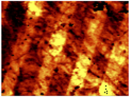
In a recent report in the journal Nature Communications, a Berkeley MSE team led by Professor Lane Martin, together with colleagues form the University of Pennsylvania and the University of Illinois, Urbana-Champaign, have found a way to control the movement and placement of electrons in graphene, and to do so in a way that can make it easy to change the polarity of the charge with an electric field. By combining graphene together with ferroelectrics, the team has demonstrated the ability to dynamically switch the nature of charge carriers in the graphene with making physical changes to the graphene. This enables non-volatile, switchable device structures (such as p-n junctions) to be produced on demand at nanometer length scales – addressing a key challenge in the widely studied 2D material graphene. The findings have implications for a range of devices including next-generation logic systems. Additional details can be found here:
Berkeley News Release: http://newscenter.berkeley.edu/2015/01/26/graphene-oxides-conductivity/
UPenn New Release: http://www.upenn.edu/pennnews/news/researchers-penn-berkeley-and-illinois-use-oxides-flip-graphene-conductivity
Contact Us
Department offices are located in 210 Hearst Memorial Mining Building, in the Northeast corner of campus.
Address:
| Department of Materials Science and Engineering | |
| 210 Hearst Memorial Mining Building University of California Berkeley, CA 94720-1760 |
Phone: (510) 642-3801 Fax: (510) 643-5792 |
