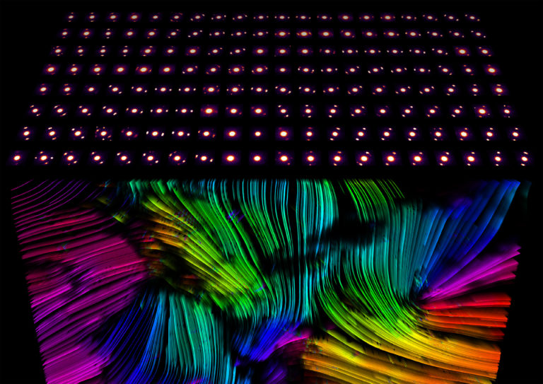
World-Leading Microscopes Take Candid Snapshots of Atoms in Their ‘Neighborhoods’

Scientists use powerful 4D-STEM electron microscopy technique to map out the best atomic ‘hangouts’ in high-performance materials. Read news story here.
Contact Us
Department offices are located in 210 Hearst Memorial Mining Building, in the Northeast corner of campus.
Address:
Department of Materials Science and Engineering
210 Hearst Memorial Mining Building
University of California
Berkeley, CA 94720-1760
Phone: (510) 642-3801
Fax: (510) 643-5792
