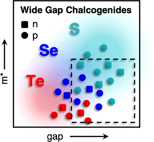
Wide Band Gap Chalcogenide Semiconductors

Scientists at UC Berkeley / Berkeley Lab (R. Woods-Robinson and K. Persson) and the National Renewable Energy Laboratory have released a comprehensive review of a unique, emerging class of materials called "wide band gap chalcogenide semiconductors". These are materials composed of chalcogen elements (sulfur, selenium, and tellurium) that are both transparent to visible light and conductive of electricity; two properties that do not commonly occur together in nature. In contrast to transparent oxides which historically get more attention, transparent chalcogenides stand out due to their unique properties and they enable new applications in a large range of energy conversion devices, such as solar cells. This article looks in-depth collectively at these materials for the first time, reviews theoretical context and state-of-the-art performance, and inspires new research directions. Read more here.
Contact Us
Department offices are located in 210 Hearst Memorial Mining Building, in the Northeast corner of campus.
Address:
| Department of Materials Science and Engineering | |
| 210 Hearst Memorial Mining Building University of California Berkeley, CA 94720-1760 |
Phone: (510) 642-3801 Fax: (510) 643-5792 |
