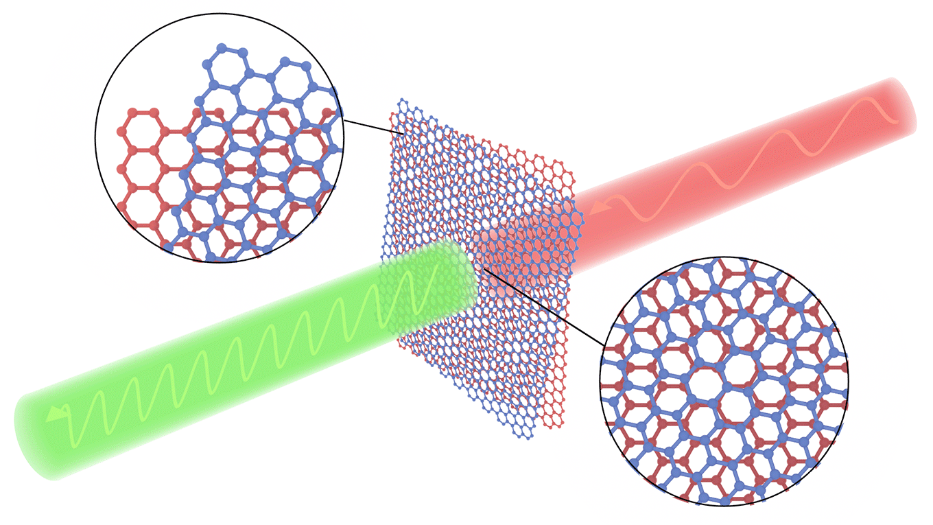
Berkeley Engineers give Graphene a New Twist to Boost Optoelectronics

As reported in the October issue of the journal Matter, researchers in our department have converted a common linear material into one with nonlinear optical capability by stacking two single-atom-thick sheets of graphene on top of each other and twisting them. The discovery relies on the strong interaction between graphene layers and the altered symmetry of atomic arrangement from the twisting. It will bring efficient nonlinear functionalities in an ultra-compact form to future photonic platforms including integrated photonic circuits. Read news story here.
Contact Us
Department offices are located in 210 Hearst Memorial Mining Building, in the Northeast corner of campus.
Address:
| Department of Materials Science and Engineering | |
| 210 Hearst Memorial Mining Building University of California Berkeley, CA 94720-1760 |
Phone: (510) 642-3801 Fax: (510) 643-5792 |
