Posts Tagged ‘Andrew Minor’
Going Cold: The Future of Electron Microscopy
Going Cold: The Future of Electron Microscopy Taking the technology to low temperatures could enable advances in materials science and other fields. Read the full interview here. Contact Us Department offices are located in 210 Hearst Memorial Mining Building, in the Northeast corner of campus. Address: Department of Materials Science and Engineering 210 Hearst Memorial Mining…
Read More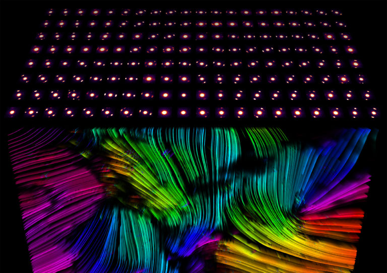
World-Leading Microscopes Take Candid Snapshots of Atoms in Their ‘Neighborhoods’
World-Leading Microscopes Take Candid Snapshots of Atoms in Their ‘Neighborhoods’ Scientists use powerful 4D-STEM electron microscopy technique to map out the best atomic ‘hangouts’ in high-performance materials. Read news story here. Contact Us Department offices are located in 210 Hearst Memorial Mining Building, in the Northeast corner of campus. Address: Department of Materials Science and…
Read More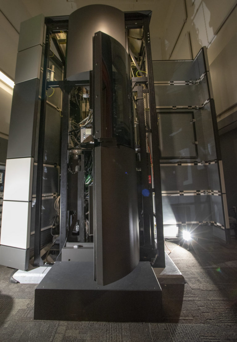
Successful Demonstration of Fastest Electron Microscopy Detector Ever Made
Successful Demonstration of Fastest Electron Microscopy Detector Ever Made by Daisy Hernandez March 7, 2019 Professors Minor and Scott participated in the team that completed the successful installation and testing of the new 4D Camera at the National Center for Electron Microscopy in the Molecular Foundry at LBNL. This camera can produce continuous electron images every 11…
Read More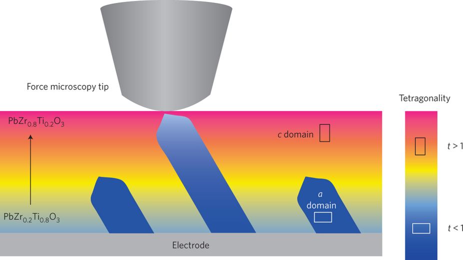
“Springy” Domain Walls featured in Nature Materials
“Springy” Domain Walls featured in Nature Materials by Daisy Hernandez April 27, 2016 A collaborative effort between MSE at Berkeley, the National Center for Electron Microscopy (NCEM) at Lawrence Berkeley National Laboratory, and the Center for Nanophase Materials Sciences (CNMS) at Oak Ridge National Laboratory identifies a pathway to produce spring-like response in ferroelectric domain…
Read More
Professor Andrew Minor Appointed Facility Director of National Center for Electron Microscopy
Professor Andrew Minor Appointed Facility Director of National Center for Electron Microscopy by Materials Science and Engineering August 5, 2015 Materials Science & Engineering Professor Oscar Dubón has been appointed as the Vice Chancellor for Equity & Inclusion at UC Berkeley. He previously served as Associate Dean for Equity & Inclusion and Student Affairs for the College…
Read More